PRODUCT VISUAL01 / GALLERY
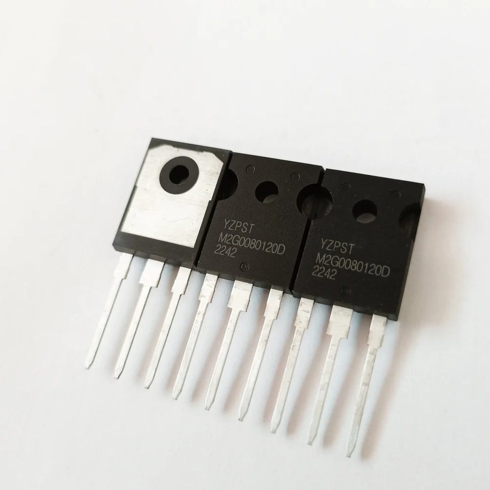
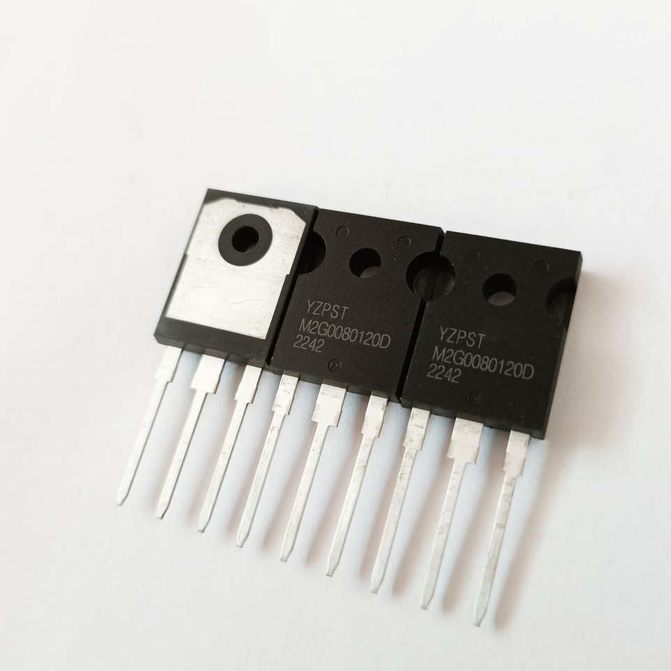
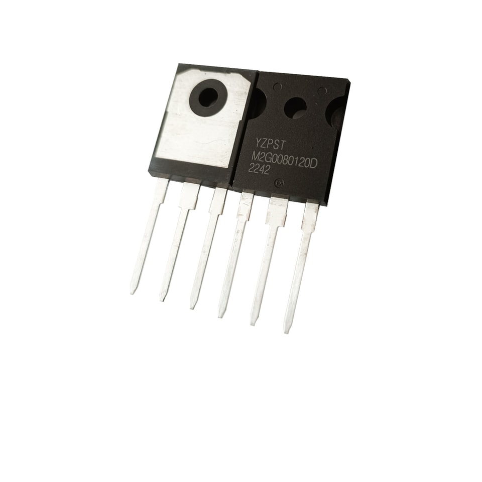
POWER COMPONENT
YZPST-M2G0080120D
✓Technical product information✓Application-focused selection support✓Catalog and requirement-based inquiry
Emailinfo@yzpst.net
Phone+86 138 0527 8321
Tip: include the part number, target voltage/current and application environment.
DOCUMENT CENTER
Downloads & technical files

1200V N-Channel Silicon Carbide Power MOSFET SiC MOSFET
FeaturesOptimized package with separate driver source pin
High blocking voltage with low on-resistance
High-speed switching with low capacitances
Fast intrinsic diode with low reverse recovery (Qrr)
Easy to parallel
RoHS compliant
Benefits
Higher System Efficiency
Reduce cooling requirements
Increased power density
Enabling higher frequency
Minimize gate ringing
Reduction of system complexity and cost
Applications
Switch Mode Power Supplies
DC/DC converters
Solar Inverters
Battery Chargers
Motor Drives
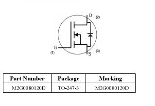
Maximum Ratings (Tc = 25 °C unless otherwise specified )
| Symbol | Parameter | Value | Unit | Test Conditions | Note |
| f^DSmax | Drain-Source Breakdown Voltage | 1200 | V | 海=0 V, /d=100 卩A | |
| Id | Continuous Drain Current | 42 | A | 4s=20 V Tc=25 °C | Fig. 18 |
| Pd | Power Dissipation | 208 | W | *=25 °C | Fig. 19 |
| FgS,op | Recommend Gate Source Voltage | -0.25 | V | ||
| J^Smax | Maximum Gate Source Voltage | -0.4 | V | AC (f>lHz) | Note 1 |
| Tj, Tstg | Operating Junction and Storage Temperature Range | -55 to | °C | ||
| 175 | |||||
| 7l | Soldering Temperature | 260 | °C |
Electrical Characteristics
| Symbol | Parameter | Min. | Typ. | Max. | Unit | Test Conditions | Note |
| Static | |||||||
| BVds | Drain-Source Breakdown Voltage | 1200 | - | - | V | 4s=0 V, Zd=100 卩A | |
| A)ss | Zero Gate Voltage Drain Current | — | 11 | 100 | 丹s=1200 V Pgs=0 V | ||
| Igss | Gate-Source Leakage | — | 10 | 250 | nA | 4s=20 V | |
| FGS(th) | Gate-Source Threshold Voltage | 2 | — | 4 | V | Id=5 mA, | Fig. 11 |
| &DS(on) | Drain-Source On-Resistance | — | 78 | 100 | mQ | 国=20 V, Zd=20 A | Fig. 6 |
| Dynamic | |||||||
| Ciss | Input Capacitance | — | 1128 | PF | 4s=0 V,比s=1000 V | Fig. 17 | |
| C^oss | Output Capacitance | — | 86 | f^l.OMHz,瓜=25 mV | |||
| Crss | Reverse Transfer Capacitance | — | 5 | ||||
| Eoss | Coss Stored Energy | - | 44 | 卩J | Fig. 16 | ||
| Qs | Total Gate Charge | — | 52 | nC | moo V | Fig. 12 | |
| figs | Gate-Source Charge | - | 17 | 血=20 A | |||
| Qgd | Gate-Drain Charge | - | 15 | Fgs=-5/+20 V | |||
| td(cn) | Turn-on Delay Time | — | 41 | ns | 丹 s=800 V | ||
| tr | Turn-on Rise Time | - | 21 | Fgs=-5/+20 V | |||
| Turn-off Delay Time | — | 48 | Id=20A | ||||
| tf | Turn-off Fall Time | — | 16 | Ro(ext)=2.5 Q | |||
| RG(int) | Internal Gate Resistance | - | 4 | n | E.O MHz, Vac=25 mV | ||
Body Diode Characteristics ,at Tj=25°C, unless otherwise noted
| Symbol | Parameter | Min. | Typ. | Max. | Unit | Test Conditions | Note |
| Is | Continuous Diode Froward Current | - | - | 42 | A | Note 1 | |
| Diode Froward Voltage | - | 4 | - | V | Kjs=0 V, Zs=10 A | Fig. 8, | |
| 9,10 | |||||||
| trr | Reverse Recovery Time | - | 26 | - | ns | 1s=20 A,既)s=800 V | |
| 0r | Reverse Recovery Charge | - | 163 | - | nC | %s=・5 V | Note 1 |
| Zrrm | Peak Reverse Recovery Current | 12 | A | di/dt=2100 A/us |
Thermal Characteristics
| Symbol | Parameter | Min. | Typ. | Max. | Unit | Note |
| Rbjc | Thermal Resistance from Junction to Case | / | 0.68 | / | °c/w | Fig. 20 |
Test Circuit Schematic

No additional product content is available.

Power semiconductor devices, protection components and industrial power solutions.
Follow YZPST


