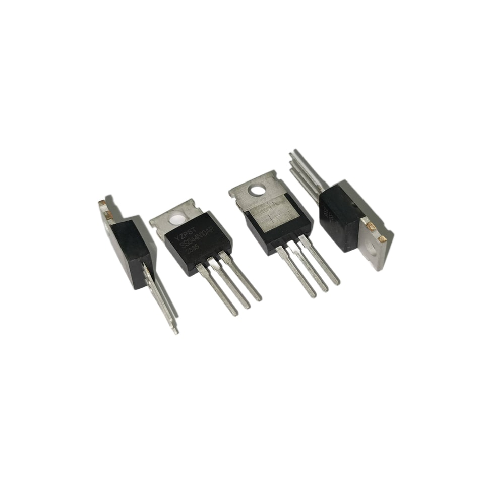
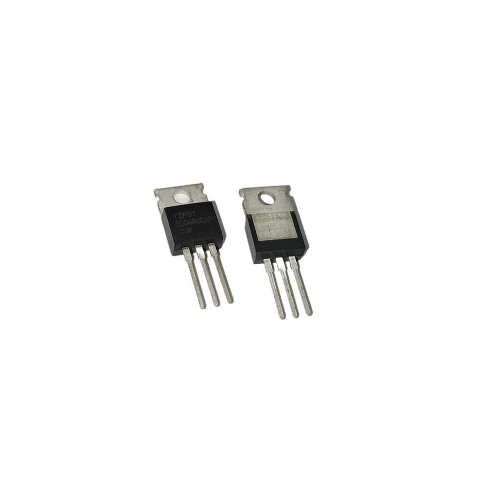
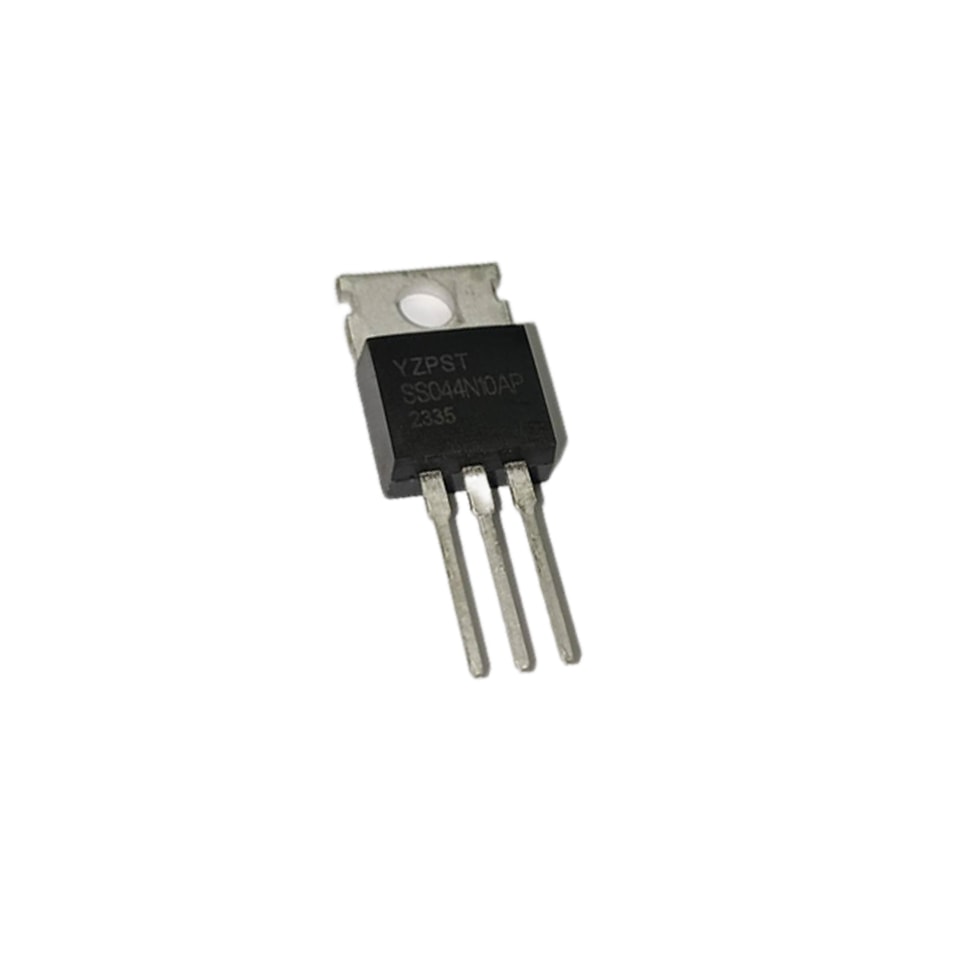
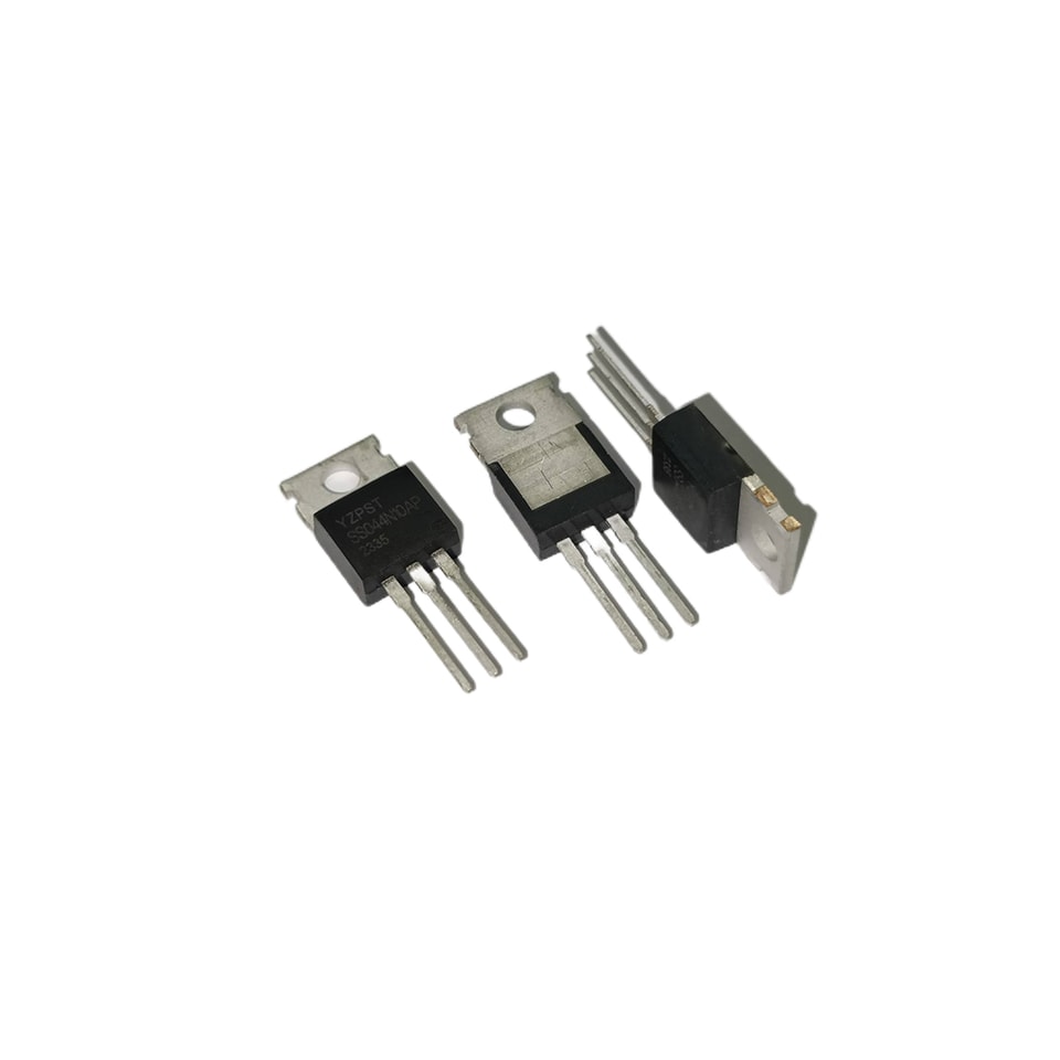
YZPST-SS044N10AP
Tip: include the part number, target voltage/current and application environment.
Downloads & technical files

100V N-Channel Super Gate Trench Power MOSFET
P/N: YZPST-SS044N10AP
FEATURES
Super TrenchFET® Power MOSFET
l100% avalanche tested
Improved dv/dt capability
APPLICATIONS
Primary Side Switch
Other Applications
Uninterruptible power supply
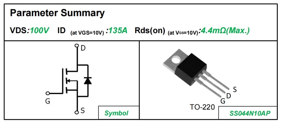
Device Ordering Marking Packing Information | |||
Ordering Number | Package | Marking | Packing |
SS044N10AP |
TO-220 | YZPST SS044N10AP |
Tube |
Absolute Maximum Ratings TC = 25ºC, unless otherwise noted | |||
Parameter |
Symbol | Value |
Unit |
TO-220 | |||
Drain-Source Voltage (VGS = 0V) | VDSS | 100 | V |
Continuous Drain Current | ID | 135 | A |
Pulsed Drain Current (note1) | IDM | 520 | A |
Gate-Source Voltage | VGSS | ±20 | V |
Single Pulse Avalanche Energy (note2) | EAS | 780 | mJ |
Power Dissipation (TC = 25ºC) | PD | 208 | W |
Operating Junction and Storage Temperature Range | TJ, Tstg | -55~+150 | ºC |
Caution: Stresses greater than those listed in the “Absolute Maximum Ratings” may cause permanent damage to the device. | |||
Thermal Resistance | |||
Parameter |
Symbol | Value |
Unit |
TO-220 | |||
Thermal Resistance, Junction-to-Case | RthJC | 0.60 | ºC/W |
Thermal Resistance, Junction-to-Ambient | RthJA | 62.5 | |
Specifications TJ = 25ºC, unless otherwise noted | ||||||
Parameter |
Symbol |
Test Conditions | Value |
Unit | ||
Min. | Typ. | Max. | ||||
Static | ||||||
Drain-Source Breakdown Voltage | V(BR)DSS | VGS = 0V, ID = 250µA | 100 | -- | -- | V |
Zero Gate Voltage Drain Current | IDSS | VDS =100, VGS = 0V, TJ = 25ºC | -- | -- | 1.0 | μA |
Gate-Source Leakage | IGSS | VGS = ±20V | -- | -- | ±100 | nA |
Gate-Source Threshold Voltage | VGS(th) | VDS = 250µA | 2.0 | -- | 4.0 | V |
Drain-Source On-Resistance (Note3) | RDS(on) | VGS = 10V, ID =50A | -- | 3.6 | 4.4 | mΩ |
Dynamic | ||||||
Input Capacitance | Ciss |
VGS = 0V, VDS = 50V, f = 1.0MHz | -- | 7300 | -- |
pF |
Output Capacitance | Coss | -- | 850 | -- | ||
Reverse Transfer Capacitance | Crss | -- | 25 | -- | ||
Total Gate Charge | Qg |
VDD = 50V, ID = 20A, VGS = 10V | -- | 114 | -- |
nC |
Gate-Source Charge | Qgs | -- | 37 | -- | ||
Gate-Drain Charge | Qgd | -- | 26 | -- | ||
Turn-on Delay Time | td(on) |
VDD = 50V, ID =50A,VGS = 10V RG =3.0 Ω | -- | 32 | -- |
ns |
Turn-on Rise Time | tr | -- | 50 | -- | ||
Turn-off Delay Time | td(off) | -- | 83 | -- | ||
Turn-off Fall Time | tf | -- | 30 | -- | ||
Drain-Source Body Diode Characteristics | ||||||
Continuous Body Diode Current | IS |
TC = 25 ºC | -- | -- | 135 |
A |
Pulsed Diode Forward Current | ISM | -- | -- | 520 | ||
Body Diode Voltage | VSD | TJ = 25ºC, ISD = 50A, VGS = 0V | -- | 0.9 | 1.2 | V |
Reverse Recovery Time | trr | VGS = 0V,IS = 50A, diF/dt =500A /μs | -- | 75 | -- | ns |
Reverse Recovery Charge | Qrr | -- | 160 | -- | nC | |
Notes
- RepetitiveRating:Pulse width limited by maximum junction temperature
- VDD = 50V,RG =25 Ω , Starting TJ = 25 ºC
- Pulse Test:Pulsewidth ≤ 300μs, Duty Cycle ≤ 1%
.jpg)
.jpg)
.jpg)
.jpg)
.jpg)

Power semiconductor devices, protection components and industrial power solutions.


